The progress of advancements in chip technology faces limitations imposed by the conventional fabrication methods of semiconducting materials employed in transistors. This obstacle to the progression of Moore's Law (stating that the number of transistors in an integrated circuit doubles about every two years) has been a long-term concern, prompting scientists to explore and develop alternative approaches in order to achieve the desired continuous improvement in chip technologies. Recently, a team of researchers from multiple institutions in the USA and South Korea has successfully overcome technical obstacles that were hindering the practical application of semiconducting two-dimensional (2D) materials, which are crucial for developing ultra-thin transistors capable of advancing Moore's Law. This achievement suggests that the mass production of top-notch 2D materials to be used in transistors is now within reach.
For the last two decades, it has been thought that one of the feasible methods for revitalizing the semiconductor industry involves the substitution of conventional silicon with 2D materials to manufacture transistors. This is mostly because of 2D materials’ numerous appealing characteristics that have been shown to greatly enhance performance, efficiency, and scalability. As an example, Intel's Components Research (CR) Group recently advocated the utilization of novel 2D materials as a pathway to developing processors with more than a trillion transistors by the year 2030.
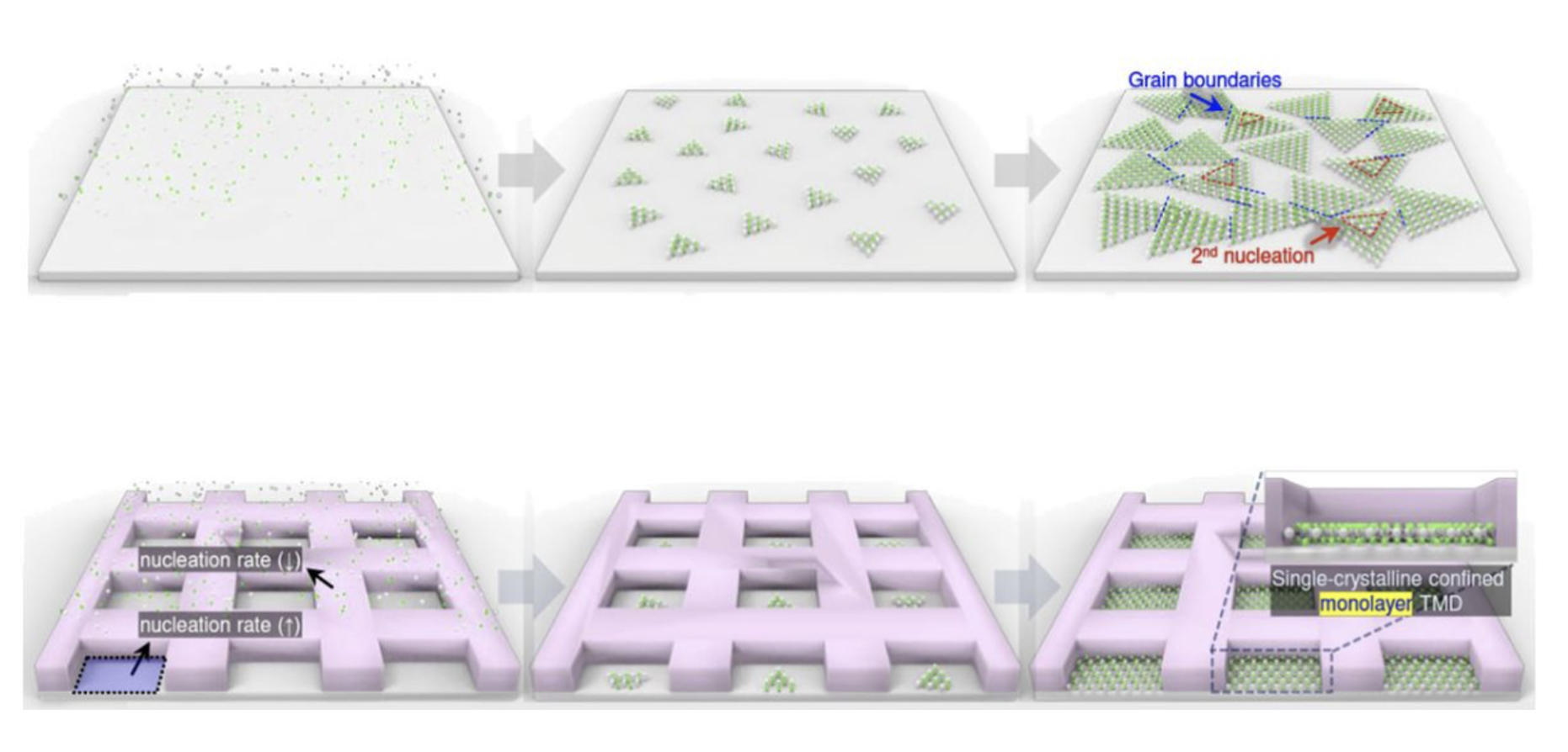
However, there has been a problem at the materials science front. Traditionally, researchers use a pseudo-manual technique to generate 2D materials, involving the delicate exfoliation of an atom-thin flake from a larger bulk material. However, the majority of bulk materials are composed of polycrystalline structures, comprising multiple crystals that grow with arbitrary orientations. At the interface where one crystal meets another, a "grain boundary" emerges, acting as an electrical barrier. When electrons traverse through one crystal and encounter a crystal with a distinct orientation, the material's conductivity is hindered. Even after successfully exfoliating a 2D flake, researchers still face the challenge of identifying "single-crystalline" regions within the flake. This endeavor is detailed, time-consuming, and hard to implement on an industrial scale.
The proposed novel approach called "nonepitaxial, single-crystalline growth" eliminates the need for the peeling and searching for 2D material flakes. Instead, they employ conventional vapor deposition (CVD) techniques to transport atoms onto a silicon wafer. These atoms then settle on the wafer's surface and initiate the growth of two-dimensional crystals. However, ordinarily, each crystal nucleus or seed would propagate in arbitrary orientations across the silicon wafer and this would create problems in manufacturing perfect 2D materials.
In order to control the geometry of crystal growth, the researchers initially applied a "mask" consisting of a layer of silicon dioxide onto a silicon wafer. The mask was carefully patterned to create small cavities, each intended to capture a crystal seed. They subsequently introduced a stream of atoms in the form of a gas onto the masked wafer, resulting in the formation of a 2D material, such as a TMD (transition metal dichalcogenide). The pockets within the mask effectively guided and confined the atoms, promoting their assembly on the silicon wafer with a consistent single-crystalline orientation.
As a result, it is now feasible to produce 2D materials in a single-crystalline state on silicon wafers. The specific challenges that were resolved can be outlined as follows:
1. Achieving accurate regulation of the growth process of 2D materials layer by layer, with precise control over the kinetics involved.
2. Ensuring the maintenance of a singular domain throughout the growth process, thereby achieving consistent thickness across the material.
3. Establishing the ability to control the layer numbers and crystallinity of the 2D material at a wafer-scale level, providing a high degree of control and uniformity.
Like any research of this kind, it may take several years before we witness the practical implementation of 2D materials. Nevertheless, given the active participation of companies such as Intel and Samsung in this endeavor, along with Intel's ongoing exploration of 2D Gate All Around (GAA) transistors, the realization of this future may arrive sooner than anticipated.
This work is detailed in the research article titled “Non-epitaxial single-crystal 2D material growth by geometric confinement” and published in Nature.
Link to original work: https://www.nature.com/articles/s41586-022-05524-0